Preface
Recently I've been trying to push ADC performance as far as possible, so I looked into the related peripheral features.
The cache and MPU attribute configuration part was something I had never fully understood before. This time I finally got it straight: on ARM chips with cache support, the cache can only be used together with the MPU peripheral configuration.
- Cache: A buffer that lets the processor core operate on memory more continuously. Since some memory operations cross buses, the cache can prefetch memory near a read hit, and delay writes to a certain degree so they can be combined into more contiguous transactions. Most importantly, it reduces internal bus contention and speeds up data processing.
- MPU (Memory Protection Unit): The memory protection unit is the ARM chip's memory protection mechanism, mainly used to configure the cache attributes of a memory region. Of course, it can be used for other things, but frankly, no one actually does. For example, when different task threads are loaded, you could configure memory regions at different granularities to emulate MMU-like behavior, but no normal person would build something that complicated.
- DMA (Direct Memory Access): It directly accesses registers and copies values in peripheral registers into memory without using processor compute cycles. After a certain amount has been copied (for example 1024), it raises an interrupt so we can process the data.
Main differences between MPU and MMU
| MPU | MMU | |
|---|---|---|
| Cache hit latency | Fixed 1 instruction cycle | 1–20 cycles |
| Management granularity | Limited number of regions (around a dozen) | Can manage RAM page by page |
| Multitasking support | Divides physical regions for limited isolation | Virtual addresses fully isolate processes |
| In plain words | For real-time applications | For Linux people |
Of course, many other chips also have cache and MPU features, but this article mainly discusses ARM chips. Their functions are similar; the difference is just management granularity, number of regions, or fixed attributes that cannot be managed. The attributes and their corresponding behaviors are all similar.
Understanding the Bus
An MCU's peripherals are distributed across different buses, and reads/writes between peripherals and memory on the same bus are relatively faster. Let's understand the bus just through the cooperation of ADC, DMA, and memory.
In my application, because DMA can only operate on peripherals and memory on the same bus, I used ADC1/2/3, DMA1/2, and BDMA1.
Read this alongside the following bus diagram. ADC1 samples with DMA1 and occupies part of the D2-domain memory; ADC3 samples with BDMA and occupies part of the D3-domain memory. After the data is initially processed, the sampled values are placed in D1-domain memory for the CPU to use in subsequent computation. This arrangement keeps cross-domain performance loss as small as possible.
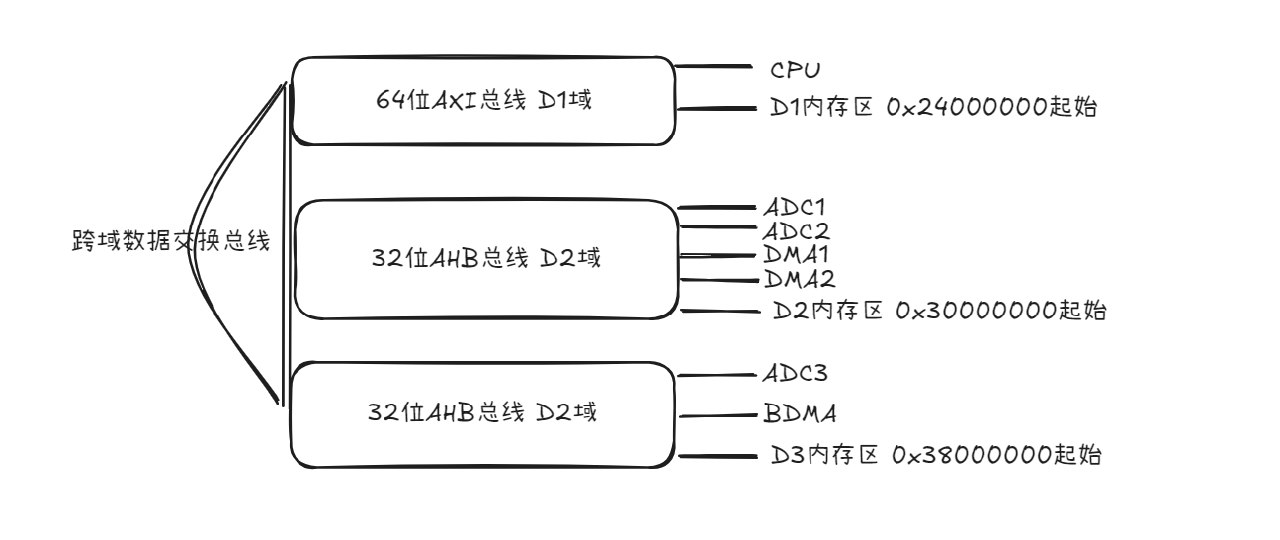
Bus diagram used
Configuring Cache Attributes
MPU configuration controls cache attributes. The three most important settings are below, along with my own brief summary:
- IsCacheable determines whether the cache is enabled.
- IsBufferable determines whether write instructions are also buffered in the cache and then written to memory as a batch. If IsCacheable is not enabled, this setting is meaningless.
- IsShareable determines whether strict timing control is used. This is very important when a peripheral accesses another peripheral's resource, such as FMC accessing external memory, because the resource is off-chip and requires strict timing.
Here is the corresponding ChatGPT explanation, which is clearer and more detailed than mine.
-IsCacheable controls whether D-Cache is used, and on M7 it works with TEX/C/B to determine the cache policy.
- IsBufferable allows write buffering/combining, which may delay the externally visible time in exchange for higher throughput.
- IsShareable marks the region as “shareable by multiple masters”; on M7 it also changes the cache policy: Cacheable + Shareable forces Write-Through/No-Write-Allocate.
Detailed explanation
- IsCacheable
- Key point: whether it goes through D-Cache; together with TEX/C/B, it determines whether the policy is Write-Back/Write-Allocate or Write-Through/No-Allocate.
- Impact: CPU access latency, bandwidth, and bus traffic; it does not directly change the peripheral sampling rate, but it affects CPU processing speed.
- IsBufferable
- Meaning: writes are allowed to enter the write buffer first and may be merged, then asynchronously flushed to memory/bus, reducing bus transactions and increasing throughput.
- Impact:
- Performance: continuous writes (memcpy, streaming writes) are faster.
- Visibility/ordering: the “visible moment” of writes to other masters (DMA/peripherals) may be delayed; use barrier instructions when necessary to guarantee ordering.
- Typical use: Normal memory is usually set to BUFFERABLE; Device/MMIO is usually not, to avoid reordering/merging.
- IsShareable
- Meaning: the region may be shared by multiple masters (CPU, DMA, etc.). On Cortex-M7 it has a special effect on Cacheable Normal regions:
- Cacheable + Shareable = Write-Through, No-Write-Allocate, which reduces the window during which other masters see stale data, but CPU-side performance is slightly lower than WB/WA.
- Cacheable + Non-shareable = usually Write-Back/Write-Allocate (with TEX=1, C=1, B=1), giving the best CPU performance.
- Impact:
- Ordering and visibility semantics are more conservative, which helps cooperation with other masters.
- This is not “hardware cache coherence”, but it changes the cache write policy and the scope of memory barrier semantics.
Quick reference for common combinations (Normal memory)
- B=1, C=1, Shareable=0, TEX=1 → Write-Back, Write-Allocate (fastest for CPU, suitable for most compute buffers)
- B=1, C=1, Shareable=1, TEX=1 → Write-Through, No-Write-Allocate (more conservative sharing semantics)
- B=0/1, C=0 → Non-cacheable (can choose whether to allow write buffering; B=0 gives stricter timing)
As shown in the earlier bus diagram, because the cache is actually part of the CPU, the memory data obtained by DMA (the D2/D3-domain memory areas) is inevitably cross-domain. In cross-domain applications, the memory consistency problem must be solved. This would require a while loop as large as the memory region to force hits and resolve consistency, which in turn causes unnecessary overhead.
Therefore, in the MPU configuration, cache is not enabled for the address ranges of the D2 and D3 domains, corresponding to the third combination above. For the commonly used memory region in the D1 domain, you can enable IsCacheable and IsBufferable and disable IsShareable to get maximum performance, corresponding to the first combination above.
As for the second combination above, I haven't encountered a use case for it yet, and I can't imagine one either.
The following code matches the above configuration. It is for reference and for my own future rollback.
/**
  * @brief MPU配置
  * @param None
  * @retval None
*/
static void MPUInit(void)
{
    MPU_Region_InitTypeDef MPU_InitStruct;

    /* 禁止 MPU */
    HAL_MPU_Disable( );

    /* 配置AXI SRAM的MPU属性为Write back, Read allocate,Write allocate
        最佳性能,用于CPU处理计算 */
    MPU_InitStruct.Enable           = MPU_REGION_ENABLE;
    MPU_InitStruct.BaseAddress      = 0x24000000;
    MPU_InitStruct.Size             = MPU_REGION_SIZE_512KB;
    MPU_InitStruct.AccessPermission = MPU_REGION_FULL_ACCESS;
    MPU_InitStruct.IsBufferable     = MPU_ACCESS_BUFFERABLE;
    MPU_InitStruct.IsCacheable      = MPU_ACCESS_CACHEABLE;
    MPU_InitStruct.IsShareable      = MPU_ACCESS_NOT_SHAREABLE;
    MPU_InitStruct.Number           = MPU_REGION_NUMBER0;
    MPU_InitStruct.TypeExtField     = MPU_TEX_LEVEL1;
    MPU_InitStruct.SubRegionDisable = 0x00;
    MPU_InitStruct.DisableExec      = MPU_INSTRUCTION_ACCESS_ENABLE;

    HAL_MPU_ConfigRegion(&MPU_InitStruct);

    /* 配置D2域MPU
        D2域外设的DMA使用 禁止cache */
    MPU_InitStruct.Enable           = MPU_REGION_ENABLE;
    MPU_InitStruct.BaseAddress      = 0x30000000;
    MPU_InitStruct.Size             = MPU_REGION_SIZE_256KB;
    MPU_InitStruct.AccessPermission = MPU_REGION_FULL_ACCESS;
    MPU_InitStruct.IsBufferable     = MPU_ACCESS_BUFFERABLE;
    MPU_InitStruct.IsCacheable      = MPU_ACCESS_NOT_CACHEABLE;
    MPU_InitStruct.IsShareable      = MPU_ACCESS_NOT_SHAREABLE;
    MPU_InitStruct.Number           = MPU_REGION_NUMBER1;
    MPU_InitStruct.TypeExtField     = MPU_TEX_LEVEL1;
    MPU_InitStruct.SubRegionDisable = 0x00;
    MPU_InitStruct.DisableExec      = MPU_INSTRUCTION_ACCESS_DISABLE;

    HAL_MPU_ConfigRegion(&MPU_InitStruct);

    /* 配置以太网收发描述符部分为Strongly Ordered */
    MPU_InitStruct.Enable           = MPU_REGION_ENABLE;
    MPU_InitStruct.BaseAddress      = 0x30040000;
    MPU_InitStruct.Size             = MPU_REGION_SIZE_32KB;
    MPU_InitStruct.AccessPermission = MPU_REGION_FULL_ACCESS;
    MPU_InitStruct.IsBufferable     = MPU_ACCESS_BUFFERABLE;
    MPU_InitStruct.IsCacheable      = MPU_ACCESS_NOT_CACHEABLE;
    MPU_InitStruct.IsShareable      = MPU_ACCESS_NOT_SHAREABLE;
    MPU_InitStruct.Number           = MPU_REGION_NUMBER2;
    MPU_InitStruct.SubRegionDisable = 0x0;
    MPU_InitStruct.TypeExtField     = MPU_TEX_LEVEL0;
    MPU_InitStruct.DisableExec      = MPU_INSTRUCTION_ACCESS_DISABLE;

    HAL_MPU_ConfigRegion(&MPU_InitStruct);

    /* 配置D3域MPU
        D3域外设的DMA使用 禁止cache */
    MPU_InitStruct.Enable           = MPU_REGION_ENABLE;
    MPU_InitStruct.BaseAddress      = 0x38000000;
    MPU_InitStruct.Size             = MPU_REGION_SIZE_64KB;
    MPU_InitStruct.AccessPermission = MPU_REGION_FULL_ACCESS;
    MPU_InitStruct.IsBufferable     = MPU_ACCESS_NOT_BUFFERABLE;
    MPU_InitStruct.IsCacheable      = MPU_ACCESS_NOT_CACHEABLE;
    MPU_InitStruct.IsShareable      = MPU_ACCESS_NOT_SHAREABLE;
    MPU_InitStruct.Number           = MPU_REGION_NUMBER3;
    MPU_InitStruct.TypeExtField     = MPU_TEX_LEVEL1;
    MPU_InitStruct.SubRegionDisable = 0x00;
    MPU_InitStruct.DisableExec      = MPU_INSTRUCTION_ACCESS_DISABLE;

    HAL_MPU_ConfigRegion(&MPU_InitStruct);

    /* 配置FMC 片选3 的支持*/
    MPU_InitStruct.Enable           = MPU_REGION_ENABLE;
    MPU_InitStruct.BaseAddress      = 0x68000000;
    MPU_InitStruct.Size             = MPU_REGION_SIZE_256B;
    MPU_InitStruct.AccessPermission = MPU_REGION_FULL_ACCESS;
    MPU_InitStruct.IsBufferable     = MPU_ACCESS_NOT_BUFFERABLE;
    MPU_InitStruct.IsCacheable      = MPU_ACCESS_NOT_CACHEABLE; // 此外设需配置为无cache,否则会重复片选和读写使能
    MPU_InitStruct.IsShareable      = MPU_ACCESS_SHAREABLE;
    MPU_InitStruct.Number           = MPU_REGION_NUMBER4;
    MPU_InitStruct.TypeExtField     = MPU_TEX_LEVEL0;
    MPU_InitStruct.SubRegionDisable = 0x00;
    MPU_InitStruct.DisableExec      = MPU_INSTRUCTION_ACCESS_ENABLE;

    HAL_MPU_ConfigRegion(&MPU_InitStruct);

    /*使能 MPU */
    HAL_MPU_Enable(MPU_PRIVILEGED_DEFAULT);
}